|
 |
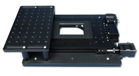
| MMP Series |
Features
- 1, 2, or 3 axis configurations
- 25mm range of motion
- Optional 50mm encoders
|
Advantages
- Proprietary intelligent control for stability
- High native precision & accuracy
- Nanopositioner compatible
|
 |
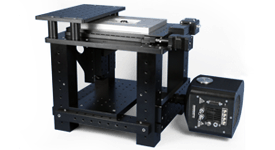
| MicroMirror TIRF System |
Features
- Integrated imaging & motion control platform
- Adjustable micromirror mounts
- TIRF lock feedback control
|
Advantages
- Optical pathway accessibility
- Eliminates dichroic mirrors
- Facilitates multiple laser lines
|
 |
|
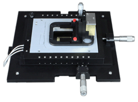
Mad-Deck™
|
Features
- XYZ motion
- High native precision and Accuracy
- Nanopositioner ready
- Optional encoders
|
Applications
- Single molecule microscopy
- Electrophysiology
- Multi Photon microscopy
- Automation
|
 | |
Nano-LPS Series : Lowest profile 3 axis nanopositioner
|
Features
- Lowest profile 3-axis piezo nanopositioner
- Large aperture for standard 3" slides
- 100 μm, 200 μm, and 300 μm ranges of motion (XYZ)
- Closed loop control
- High stability
|
Applications
- Optical microscopy, easy to retrofit
- Optical trapping experiments
- Fluorescence imaging
- Alignment
- Single molecule spectroscopy
- Super resolution microscopy
|
 |
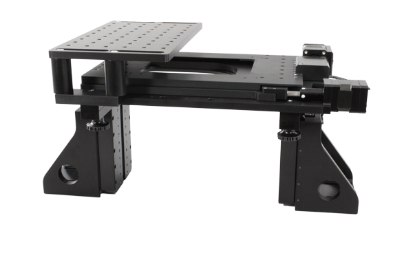
| RM21™ Microscope Platform |
Features
- Designed for maximum user accessibility
- Manufactured with high precision to allow easy alignment of microscopy and optical components
- Robust design
- Precision manufacturing and assembly
|
Applications
- Particle tracking
- Fluorescence microscopy
- TIRF
|
|
|
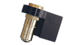
Nano-F Series: High precision lens positioners |
Features
- Compact objective lens piezo stage
- Interchangeable, quick mount adapters
- 100 μm or 200 μm ranges of motion
- Compatible with all microscopes
- Closed loop control
|
Applications
- Microscope focusing element
- Confocal imaging
- Auto focus
- STORM and PALM imaging
- Light sheet microscopy
|
|
| MCL-MOTNZ: Low cost, high performance microscopy stage |
Features
- Integrated 1" [25mm] micropositioner and Z axis closed loop nanopositioner
- Holders for slides and 35mm dishes
- Fits inverted optical microscopes and optical tables
|
Applications
- Optical microscopy, easy to retrofit
- Confocal imaging
- Fluorescence imaging
- Single molecule spectroscopy
- Nanomanipulation
- STORM and PALM imaging
|
RM21™ Imaging Platform |
|
 RM21™ is piezo nanopositioner ready. It is a precision aligned imaging platform designed for maximum user accessibility. This feature offers users the opportunity to develop flexible configuration microscopy instruments that integrate nanopositioning systems with ease. It has been manufactured with high precision to allow easy alignment of microscopy and optical components within its three dimensional space. In addition, all posts and fixturing points are referenced to a known datum. With a robust design, precision manufacturing and assembly, the RM21™ is the ideal platform for a range of microscopy applications such as super resolution (SR) microscopy, fluorescence microscopy and TIRF. RM21™ is piezo nanopositioner ready. It is a precision aligned imaging platform designed for maximum user accessibility. This feature offers users the opportunity to develop flexible configuration microscopy instruments that integrate nanopositioning systems with ease. It has been manufactured with high precision to allow easy alignment of microscopy and optical components within its three dimensional space. In addition, all posts and fixturing points are referenced to a known datum. With a robust design, precision manufacturing and assembly, the RM21™ is the ideal platform for a range of microscopy applications such as super resolution (SR) microscopy, fluorescence microscopy and TIRF. |
| We use Clicky Web Analytics to log and analyze the traffic to our web site. You may review Clicky's privacy policy here. We log "personal data" to Clicky as follows, for the stated legitimate purposes. A "Unique ID" tracking cookie to identify unique visitors, your IP address for security and fraud prevention. |
Applications |
Mad City Labs, Inc piezo nanopositioning systems, micropositioning systems, instrument solutions, and piezoactuators are used for a variety of applications. The following categories represent a few of the most popular applications for nanopositioners and nanopositioning systems.
|
 |
Image at left: SR microscopy (STORM) image of Cy5-Cy3 labeled tubulin from A431 cells, courtesy of Prof. K. Lidke, University of New Mexico.
Super-resolution microscopy is a blanket term used to describe several newly emerging forms of light microscopy, each of which surpasses the classical diffraction limit as described by Ernst Abbe. While conventional light microscopy attains resolving power of about 250nm, these SR techniques enable resolutions of tens of nanometers.
The SR methods depend on photo-physical properties displayed by particular fluorescent probes used to mark the particular process of interest. The fluorescent state of these probes can be proactively manipulated by exposure to specific wavelengths of light. SR microscopy exploits these probe properties to either spatially restrict (STED, SSIM), or temporally separate (STORM, PALM) the photons emitted by two closely spaced fluorescent sources so that they can be imaged separately, and in doing so circumvents the diffraction limit.
The SR methods show great promise to enable unprecedented views into the dynamic world of the cell at the nanometer scale. However, these SR imaging techniques place a great premium on the stability of the imaging system, and as the SR methods make their way into common use, a “stability limit” may replace the diffraction limit on resolving power.
Mad City Labs offers several products designed to achieve ultra-high stability in an imaging system through active feedback compensation of measured system drift.
|
|
|
 |
Fluorescence Microscopy & Spectroscopy
Image at left from Valeria Levi, Anna S Serpinskaya, Enrico Gratton, and Vladimir I Gelfand. Organelle transport along microtubules in Xenopus melanophores: evidence for cooperation between multiple motors. Biophys J. 2006; 90(1): 318-27. Figure 5(c)
|
Mad City Labs' multi-axis piezo nanopositioning sample stages, objective lens piezo nanopositioners, micropositioning stages, and C-Focus microscope stabilization system are being used for fluorescence detection techniques including Förster resonance energy transfer (FRET) imaging, fluorescence lifetime imaging microscopy (FLIM), confocal microscopy, coherent anti-Stokes Raman spectroscopy (CARS), total internal reflection fluorescence (TIRF) imaging, fluorescence recovery after photobleaching (FRAP) imaging, and others.
|
|
|
 |
Scanning Probe Microscopy & Surface Profilometry
Image at left generated from Data taken using MadPLL™ with Nano-OP30 nanopositioning system (Z-axis), Nano-OP100 nanopositioning system (XY axes): Fly eye, 100µm x 100µm bidirectional scan, PLL mode, constant probe signal, Z force feedback: frequency.
Scanning Probe Microscopy (SPM) refers to a category of microscopy techniques that form images of surfaces using a physical probe that scans a sample. Examples of commonly used probes are tungsten tips and the Akiyama probe. An image of the surface is obtained by mechanically moving the probe in a raster scan of the sample and recording the probe-surface interaction as a function of position. Atomic, and even sub-atomic, resolution can be achieved by many SPM techniques largely due to the characteristics of the piezo-actuated motion control used in SPM instruments.
Mad City Labs offers a high-resolution, closed loop piezo nanopositioning systems well suited to atomic force microscopy (AFM), near field scanning optical microscopy (NSOM), and other SPM applications. Our recently developed product, MadPLL®, offers users the ability to assemble a robust, inexpensive SPM system for use in a variety of environments.
For additional information about building an SPM with Mad City Labs systems, visit the SPM-M Kit, MadPLL®, and AFM Video Tutorial pages and the Laser Focus World article NANOPOSITIONING: Piezoelectric nanopositioners forge low-cost atomic force microscope.
|
|
|
 |
Optical Tweezers & Optical Traps
Image at left from Wang, S., Arellano-Santoyo, H., Combs, P.A., Shaevitz, J.W. Actin-like cytoskeleton contributes to cell mechanics in bacteria. Proc. Natl. Acad. Sci. 107(20):9182-9185 (2010). Figure 1(b).
Optical tweezers are capable of manipulating nanometer and micrometer-sized dielectric particles by exerting extremely small (piconewton) forces via a highly focused laser beam. Optical traps are very sensitive instruments and are capable of the manipulation and detection of sub-nanometer displacements for sub-micron dielectric particles. (Ref. Moffitt JR, Chemla YR, Izhaky D, Bustamante C [2006]. Differential detection of dual traps improves the spatial resolution of optical tweezers. Proc. Natl. Acad. Sci. U.S.A. 103 (24): 9006–9011.) They have been used to manipulate and study single molecules by interacting with a bead that has been attached to that molecule. DNA and the proteins and enzymes that interact with it have been studied in this way.
Most optical traps are operated such that the dielectric particle rarely moves far from the trap center. The reason for this is that the force applied to the particle is linear with respect to its displacement from the center of the trap provided the displacement is small. In this way, an optical trap can be compared to a simple spring, which follows Hooke's law. The particle position can be maintained by either precisely moving the sample or moving the trap itself.
Mad City Labs produces piezo nanopositioning systems with sub-nanometer precision that enable the particle to remain centered and beam steering nanopositioning systems which can control the laser beam path and hence the location of the optical trap.
|
|
|
 |
Magnetic Tweezers, Magnetic Traps, & Magnetic Manipulation
Image at left from Fisher, J.K., J. Cribb, K.V. Desai, L. Vicci, B. Wilde, K. Keller, R.M. Taylor, J. Haase, K. Bloom, E.T. O'Brien, and R. Superfine. Thin-foil magnetic force system for high-numerical-aperture microscopy. Rev Sci Instrum. 2006. 77(2): 023702-1–023702-9. Figure 8 [inset].
|
Mad City Labs offers single and multi-axis piezo nanopositioning systems for magnetic tweezers, magnetic traps, and magnetic manipulation. Our product line consists of piezo stages with many different form factors and features, including high speed systems, systems with apertures, and systems for high force or load.
|
|
|
 |
Nanofabrication, Nanopatterning, and Nanomachining
Image at left of 100µm square pattern created by modification of glass structure by non-linear absorption of femtosecond laser, courtesy of Y. Bellouard and Femtoprint.
|
Mad City Labs piezo nanopositioning systems and micropositioing systems are used for nanofabrication, nanopatterning, and nanomachining. The Nano-Align3 Series, Nano-Align5 Series, and Nano-Align6 Series provide multiple axes of linear positioning along with multiple axes of tip, tilt, or rotation to make parallel alignment with nanometer precision possible for accurate alignment and positioning. Mad City Labs also manufactures high speed and high load systems for special applications.
|
|
|
 |
Other Applications
Image at left from Myun-Sik Kim, Toralf Scharf, and Hans Peter Herzig. Small-size microlens characterization by multiwavelength high-resolution interference microscopy. Opt. Express 18, 14319-14329, 2010. Figure 4(a).
| Mad City Labs'piezo nanopositioning systems, micropositioning systems, integrated systems, and instrument solutions have been used for a variety of other applications. A small sampling of these applications includes Optical Antennas and Nano-Optics, High Throughput Imaging, Phase Shift Interferometry, Particle Accelerator Beam Profiling, Active and Adaptive Optics, Lithography, and MEMS and NEMS testing.
|
|
|
|